Over the last decade, little has changed as far as video card memory technology is concerned. However, with the introduction of the High Bandwidth Memory by AMD, a lot of changes are expected.
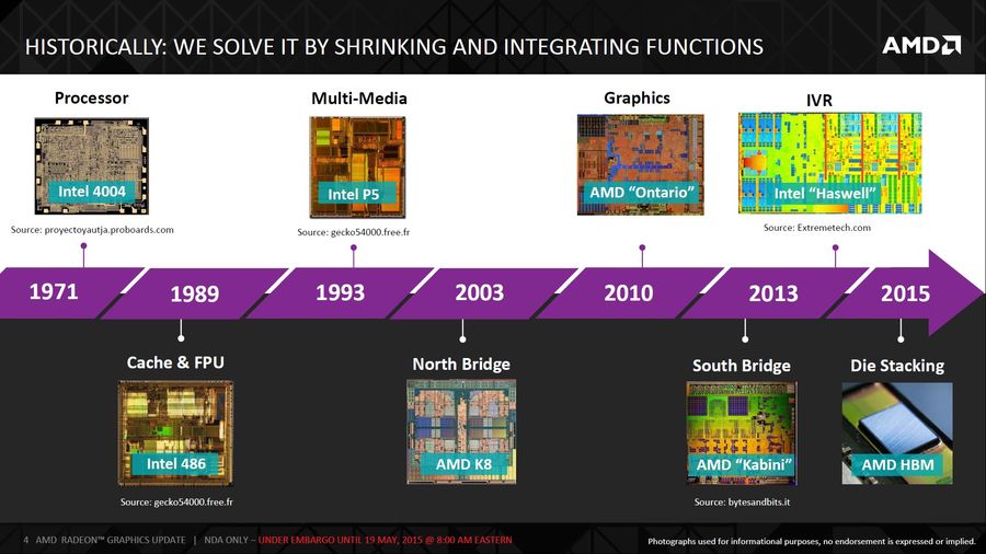
For several years now, AMD has been on the front line in the development of new forms of memory for use in graphic cards. In 2011, the company in collaboration with Hynix (now SK Hynix) announced their plans to develop High Bandwidth Memory (HBM), which was meant to set the next generation memory standards.
Four years later and the experimentation seems to have materialized. Earlier this month, AMD announced that they would be releasing their inaugural HBM-equipped GPU to the retail market this quarter. This will mean that the reign of the current market leader, GDDR5, is nearing its end-life.
The entry of High Bandwidth Memory will help provide solutions to the various drawbacks that GDDR5 has always had, and which have been a source of concerns for many users. While AMD has yet to release the full details of their forthcoming HBM-equipped GPU, it has provided some information on what to expect once HBM is launched.
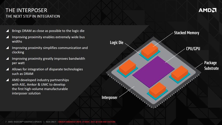
HBM has three crucial constituents; a main chip (which is either a SoC, GPU or CPU), one or several DRAM stacks, as well as a silicon wafer referred to as an interposer.
A Silicon Interposer
The interposer is an underlying silicon die that located beneath the DRAM stacks and the main chip. It is entirely passive in that it lacks active transistors since it only serves as an interconnect path between the DRAM stacks and the primary logic chip. The interposer facilitates a close integration between the HBM’s GPU and the DRAM. This enhances the HBM’s speed since all the communication between the memory and the GPU takes place across the interposer. Made of silicon, the interposer is denser than the conventional off-chip package, which enables it to accommodate an increased number of connections and traces.
Stacked memory
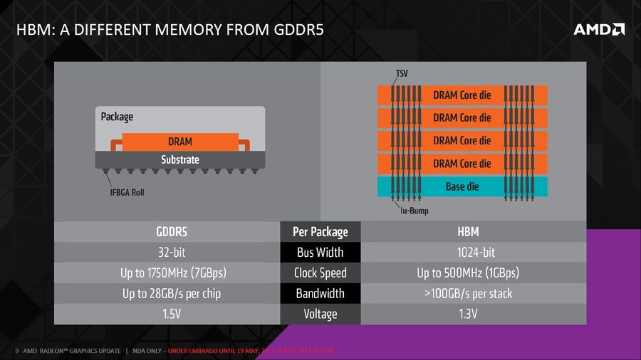
In addition to the brilliant interposer in AMD’s High Bandwidth Memory, perhaps the most interesting innovation in the HBM setup is the stacked memory. Each memory stack comprises five chips. This entails four storage dies that lie above a solitary die that controls them. The five chips are interconnected to each other using some vertical connections referred to as the through-silicon vias (TSVs). These pathways have been created by drilling a hole that passes through the silicon layers of the incredibly thin storage chips. The “microbumps” or μbumps are the metal bits positioned between the stack layers, and which help provide a comparatively shorter conduit from the logic die to all other layers of the storage cells.
A wide interface
In order to take advantage of the HBM’s distinctive layout, each of the storage dies comes with a new memory type. This memory runs at lower voltages compared to GDDR5 (1.3V compared to the 1.5V for GDDR5). Additionally, it has lesser clock speeds (500MHz versus 1759MHz) and slower transfer rates (1 Gbps versus 7 Gbps for GDDR5). However, HBM makes up for all these attributes by including a remarkably wide interface. This will see HBM include two 128-bit-wide channels for each DRAM die in the stack. On the other hand, each stack will have a combined interface width of 1024 bits which is a massive improvement from the 32 bits for the GDDR5. Thereby, at 1 Gbps, HBM will have 128 GB/s of bandwidth for each memory stick.
Conclusion
The innovation has majorly been a collaborative effort between AMD and other partners. However, AMD carried out much of the initial designing of the interposer and the improved DRAM type. Other industry players such as Hynix, UMC and JEDEC partnered with the company in coming up with the final product. To this end, AMD has yet to confirm anything else about the upcoming video cards. The technology is expected to appear only on flagship cards at the start before being distributed fully in the market.



















![[Review] Logitech G502 Lightspeed: Any Good for Gaming? 20210322 170539](https://performancepsu.com/wp-content/uploads/2021/03/20210322_170539-201x113.jpg)


